
Silkscreen in PCB Board Fabrication
Silkscreen is a key component of PCB board fabrication that is used to print all the necessary information required for the assembly process. It can be printed in various colors and font sizes to provide a clear and concise view of the circuit board. The purpose of silk screen printing is to help in reducing both the time taken for assembly and rework, as well as to improve the quality of the finished product. It can also reduce manufacturing costs by allowing for more components to be fitted on the same PCB surface area, which can save on both material and labor costs.
Before the actual production of the PCB, the board must undergo a design review, known as Design for Manufacturability (DFM) check, to ensure that the layout of the circuit meets all the required specifications and tolerances. This is to ensure that the design will be able to function as intended and is not subject to any problems during the fabrication process.
Once the DFM review is complete, the pcb board fabrication is then ready to start the fabrication process. The first step is to apply the PCB design onto the material layers, using laser direct imaging. This provides photo negatives of the board layout, which will serve as a guide during each manufacturing stage.
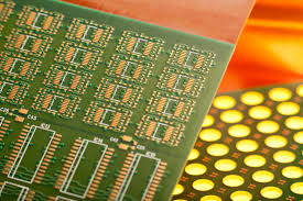
What Is Silkscreen in PCB Board Fabrication?
The next step is drilling the holes required for the connections between the different layers. The holes are then plated with copper, forming conductive pathways between the component pads and traces on the surface of the PCB. Once the drilling and copper plating are completed, the remaining tin layer is chemically stripped off the copper, leaving only the pattern and pad locations.
Finally, the silkscreen legends are printed on the bare circuit board using one of the following methods:
Manual screen printing (PSP): PSP is the most common method for printing PCB silkscreens, and is typically used for boards with large areas of text or with a high level of precision. A stencil is used to create the desired pattern on the board, and ink is applied through this stencil. The exposed parts of the stencil are then hardened by UV exposure, forming the legends on the PCB. The unexposed parts of the stencil remain unhardened and are washed away in the developing process.
Liquid Photo-Imaging (LPI): LPI is a more precise method of printing that does not require the use of stencils. Instead, the PCB is directly printed with ink based on the digital design files.
After the silkscreen printing is done, the PCB must be passed through an inspection procedure to confirm that the printed information is accurate and consistent with the design files. This includes checking for component identifiers, polarity markings, test points, and other critical information. In addition, it is important to ensure that the silkscreen follows industry standards for character size, line width, spacing, and positioning. This is to prevent mistakes that could cause serious consequences during assembly and rework.