
Steps Involved in Prototyping a Circuit Board
The first step involves conceptualizing the design and drawing it. This is often done on a piece of paper or using Electronic Design Automation (EDA) software, and it represents the overall layout with the components and their basic connections. This is the most important stage of a circuit board’s design. Without a well-thought-out schematic, the board’s functionality cannot be determined.
Next, the schematic diagram is converted into a netlist, which is a computer file that contains all the component locations and their electrical connection details. This is a very important step as it is what the manufacturing files are based on. The final file is then converted into the Gerber format, which is the industry standard for PCB fabrication and assembly. The file also contains a Bill of Materials, which lists the components that will be used for the project.
A layer stack is then created, along with any impedance profiles that may be needed. This is a crucial part of the circuit board design process because it determines what routing styles can be used. Different routing styles will enforce different trace widths, which in turn affect the impedance of a signal. This is why it is important to have an accurate impedance solver that works for all of the routing styles in your design.
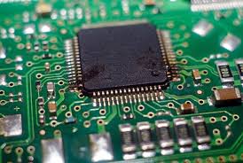
What Are the Steps Involved in Prototyping a Circuit Board?
After the layer stack and impedance profiles are set, it’s time to start placing components on the board. This step is a good opportunity to double check that all of the mechanical elements are in the right place and that all of the traces have been properly routed. This is also the time to add any labels, identifiers, or markings that will aid in the assembly and testing of the finished board.
Once all of the components are placed on the board, it’s time to solder it together. This is a complicated process that requires skill and precision to ensure the leads from each component are correctly connected to their corresponding traces on the PCB. During this stage, it’s important to pay close attention to the component manufacturers’ guidelines for placement and to avoid crossing or shorting any connections.
Once the soldering is complete, it’s a good idea to run several electrical tests on the board to ensure that all of the components are functioning properly. These tests can include visual inspection, functional testing, and automated optical inspection.
These tests will help to identify any defects or errors in the board before it goes into production. This helps to prevent costly mistakes that could ruin the board or the project as a whole. If any of the test results come back unsatisfactory, it’s a good idea to redesign the circuit board before continuing with assembly and manufacturing.